Showing posts with label RF Signal Source. Show all posts

18 September 2016

Revisit AD8307 Power Meter Calibration

This year at our club, annual pig picking BBQ and show-n-tell I had a chance to borrow the kind services of fellow Knightlites member OM John, KU4AF and his brand new and beautiful digital spectrum analyzer.

Connecting the Si570 based oscillator from my Sweeperino   into the Spectrum Analyzer and measuring the power level of the fundamental frequency we measured a -4dB difference in power when compared to measuring the squarewave on the AD8307 based wideband (~500MHz) Power Meter. Using a Low Pass Filter to filter out the odd numbered harmonics I resolved to measure the power in the fundamental on my work bench.

For the experiment I used the well known 10MHz calibration source as developed by K3NHI. This source can be used to establish the -10dBm point on the power meter through the measurement of a DC voltage level at the DC port. This reference is easy to build and is recommended for any homebrew starting out with a basic 50 Ohm bench.

Indeed my result showed a 4.1dB difference in power reading of the fundamental vs the wideband signal.

Herewith below are my Lab Notes of the procedure adopted.


11 April 2014

Rf signal source. Return Loss tests

Following up from my previous blog I was puzzled as to why the level had dropped from the initial tests of 16dBm to around 7dBm. On further inspection I discovered that the 220 Ohm resistor was still in place across the buffer amplifier broadband transformer!

The lesson learnt here being.....if there is an unexplained test then believe the test and investigate...as to why!

On removing the resistor the Return Loss was re-measured. Refer to lab notes for details. I was very pleased to see that the RL now was measured at 21dB. Definitely a good news story!.

Output power was measured as follows:

at f= 6651KHz = 15.36dBm.

I perceived that this was off the scale of the power meter so a 20dB attenuator was added. This derived a power output of 16.2dBm. Indeed, the above measurement was off the scale of the Power Meter.

Next inserted a 30dB pad and the output was derived at 16.1dBm. This output is 9dB higher than expected. Why? The output amp does run hot. Do calcs for the output amp to check the collector current.

A quick check of linearity. (Using a 30dB pad).

Fmin = -15.6dBm
Fmax = -13.95Bm
Change over the range = 1.65dB. This is good.

Next complete the inclusion of the bandspread caps and check frequency stability of the oscillator.


10 April 2014

RF Signal Source. Amplifier stage 1

I now build the amplifier stage for my homebrew RF signal source as per EMRFD Fig 7.27. The schematic is shown in the lab notes below. This stage uses a 2N3866 transistor as the amplifier with a standard 4:1 broadband transformer in the collector. A 3dB pad is inserted in the output to improve Return Loss. Some signal is fed off to a separate port for connection to a frequency counter. The build came together easily after about 45 minutes construction time UGLY style! No issues with getting the stage to work.

Initial quick tests showed an output of 12.3dBm. However subsequent more careful tests showed the output as follows which are more in line with expectations.

Fmax at 1381KHz output = 7.4 dBm
Fmin at 2783KHz output = 5.67 dBm

Why is the output higher for the higher frequencies than the lower frequencies? Investigate further.. Is 2 dB difference over the frequency range in line with expectations?

The oscillator tank circuit was shorted out to test the total system RL which = 18dB. This is a satisfactory result although not stellar.

The RL was then measured with the tank circuit running at an offset frequency (3243KHz) as opposed to the test frequency of 7022KHz. This did not work indicating a negative RL.

The amplifier stage was then disconnected from the buffer and terminated in 50 Ohms across the base 330 Ohm resistor. This did not work as the RL was low.

The 50 Ohm termination was then moved to the input of the 3dB pad. This worked and resulted in a RL of 18dB.

Referring to the previous blog on buffer stage testing, this result was revealing. The buffer RL tests showed a poor 5dB RL. However when the buffer stage is connected to the amplifier the RL output is an acceptable 18dB. This RL figure is exactly the same as that obtained when the amplifier stage was tested in isolation with it's input terminated in 50 Ohms. Why is this? Perhaps there is an error in the procedure used to measure the RL of the buffer stage in isolation?


RF Signal source. Buffer stage measurements 2

Following on from my last blog I next worked to try to measure the Return Loss, RL, of the buffer stage. This was not so easy. Some notes as follows.

Refer to the below schematic of the test configuration using the MFJ259B as the signal source into the Return Loss Bridge with a 6dB PAD. The objective was to measure the output Return Loss of the buffer amplifier.

With the oscillator connected to the buffer stage and the oscillator tank circuit short circuited (to disable the oscillator), the Return Loss (RL) was measured at 5.48dB which is very low. The target being to achieve better than at least 18dB. This being an SWR of 1.2:1.

Next the input to the buffer was terminated in 50 Ohms with the oscillator disconnected. The RL measured remained unchanged. Turning the stage power on/off had no effect. Shorting the input to the buffer had no effect.

The 3dB Pad was disconnected from the broadband transformer and terminated in 50 Ohms. This gave a better RL of 26dB. Indicating that the 3dB pad is working.

The 4:1 broadband transformer was reconnected to the Pad but disconnected from the JFET collector. RL= 5dB. The transformer was then terminated in a 200 Ohm resistor. RL = 26dB, Good! This showed that the broadband transformer was working at the test frequency of 7020KHz. The RL remained at 26dB when the transformer was connected back in the collector circuit with the 200 Ohm resistor in place. RL remained unaffected by the stage being turned on. The output however dropped from -5.7dBm with no 200 ohm resistor to -11.45dBm with the resistor in place.

OBSERVATIONS
The output RL was completely unaffected by any change to the terminated input impedance. Perhaps this comes as no surprise because the input impedance into the emitter is very low at a calculated value of 2.3 Ohms. Thus to get an input match would be very difficult.

In order to get an acceptable stage output RL the broadband 4:1 transformer must be terminated in a 200 Ohm resistor on the primary side, however at the expense of a loss of output signal level. This since half the power developed in the collector is being dissipated in the 200 Ohm resistor.

At the end of the day perhaps it does not matter if the RL is high from the buffer since the objective is to ensure high Reverse Isolation and not amplification. But what about harmonic distortion introduced in the stage? Is that of concern? The stage appears to be working correctly in spite of the high return loss.

ERROR NOTES
In the lab notes below the RL is shown as dBm. This is incorrect. RL is expressed in dB.


09 April 2014

RF signal source. Buffer stage measurements

Making measurements on the RF signal source buffer stage would be a good learning opportunity. The RF signal source as per EMRFD Fig 7.27 deploys a Common Base Amplifier using a 2N3904 transistor and a 4:1 broadband transformer in the collector. Refer to the schematic below. The output is then terminated in a 3dB pad before connecting to the power amplifier stage. The function of the stage is to create high reverse isolation so that the oscillator frequency will not 'pull' based on changes to the output load.

I analyzed the circuit using equations presented in Chapter 2 of EMRFD. Essentially the stage has unity current gain. The input to the stage is derived as a current source since the emitter input impedance is very low. This being the reason for the high reverse isolation characteristics. Thus it is a challenge to drive power into the stage. Using a theoretical Voltage gain of 200, I was unable to measure that much voltage gain. However using a unity current gain model, the measured and calculated output power correlated.

The open circuit oscillator output voltage was measured using a 10X scope probe. The stage Vin was then measured with the buffer connected. Using a simple small signal model to derive the stage input impedance (222 Ohms), the oscillator source impedance of 25.9 Ohms  was derived. Should this in fact be 50 Ohms (to be investigated). I assume that this is not critical since the oscillator stage is lightly coupled to the buffer stage through a 220 Ohm series resistor.

Some results are presented as follows:

Vcc = 12.17V
Ftest = 2825.09KHz
Ie (emitter quiescent current) calculated = 11mA (I used the long equation 2.11 EMRFD for this calc)
Ve (emitter quiescent voltage) calculated = 2.97V, measured = 2.8V
Ve (base quiescent voltage) calculated = 3.57V, measured = 3.45V
gm (transconductance) calculated = 0.4231, Rin (emitter) = 1/gm = 2.36 Ohms
Rl (collector load resistance) calculated = 200 Ohms.
Vosc open circuit = 960mVp-p
Vin = 860mVp-p
Rin (stage) calculated = 222.4 Ohms.
Rsource oscillator calculated = 25.9 Ohms.
Ib (base current) = 3.86mA
Power output in collector calculated based on voltage gain = 2mW (+3dBm)
Power output in collector calculated using unity current gain = 0.38mW (-4dBm)
Power output in collector measured (v*v/8R) = 0.38mW (-4dBm)
Power output after 3dB pad = -7dBm

All 'in situ' measurements were made using a 10X scope probe. Output power measurments at 50 Ohms were made using the RF power meter or by using the scope connected through a 50 Ohm thru terminator.

Next the stage input and output Return Loss, Power Gain and Reverse Isolation will be measured.


03 April 2014

RF signal source. Prototype build and test 2.

I have now rerouted the main variable capacitor wire away from the bandspread capacitor wire. This issue is now fixed. Next I replaced the 10pf blocking capacitor with a 6.8pf capacitor. No real difference seen in performance.

The inductor was also rewound using much tighter turns in an effort to try to improve stability. When I reinserted it back in the circuit the drift was far worse than the more loosely wound inductor. After doing some reading it was noted that often it takes time for coils to settle down due to stress in the wire caused by tight winding. I then boiled the inductor in boiling water for a few minutes. This appeared to have stabilized the coil.

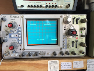
I then changed out the JFET MPF102 for a J310. This resulted in a very distorted waveform (see pic). My assumption was that this was caused by some parasitic oscillation. I noted that the output voltage was in fact similar to the MPF102. Upon changing back to the MPF102 the waveform was once again clean. No further investigation carried out.

Next I made some measurements of Time, vs Temperature, Vdd and Frequency. I left the circuit powered on for a few minutes before beginning the tests so as to not measure warm up drift. The shack temperature varied between 23.5C and 23.4C with a stable Vd-d = 12.12V. The frequency varied between 7007430Hz and 7007404Hz according to my frequency counter. A variation of 26Hz. More tests over a wider temperature range needed once the buffer and amplifier stages are built.

Next steps: Build the buffer stage.
Waveform showing distortion when a J310 was deployed. Is this parasitic oscillation occurring?

Thermal stability tests. A wider range in temperature is needed to measure frequency stability correctly.

02 April 2014

RF signal source. Oscillator prototype build & test

I am in the process of building an RF Signal Source as per EMRFD Fig 2.27. This is a Hartley design and incorporates 2 oscillators. The first covering a nominal 2-10MHz and the second covering a nominal 10-45MHz.

The Hartley topology is chosen for two reasons. a) The capacitor in the resonator can be fully variable and thus allows a wide range of frequency coverage unlike the Colpitts where, by definition, the feedback capacitors are fixed. b) The oscillator exhibits a reasonably flat output power over a wide frequency range.

Having built the chassis, installed the variable capacitors and cut the panels for the enclosure, I was now in a position to build a rough prototype of one of the oscillators. I chose the lower frequency oscillator. This took me a few hours to build. Since I don't have any of the specified 2N4416 JFETS, I decided to start with an MPF102. I selected sample 2 (Ref JFET experiments blog)  since it had a lower pinch-off voltage and higher Idss than sample 1, although not as good in performance as the tested J310. I decided to start with just the 400pf variable capacitor. This should allow easier troubleshooting since there are fewer parts. (refer to the schematic attached).

The oscillator powered up first time with no issues. The oscillator turn on voltage Vdd was 1.96V. Maximum output was obtained with a Vdd of 7.58V. Thus there was an excess of current flowing in the drain as Vdd was increased to 12V. The scope output waveform 'looks' clean. I have no way of measuring the harmonic distortion. Could increasing the rail voltage beyond 7.58V result in an increase of harmonic distortion?

The 3 turn link output was first terminated in a 50 ohm feed thru connector which was connected to the scope channel 1. This channel is also fed to the frequency counter. Then the output was connected to the Power Meter.

The oscillator is reasonably stable and certainly acceptable for general measurements and can be improved upon with more careful construction. Measuring at a frequency of 7030.44kHz and starting at 08:30 am the oscillator drifted upwards to 7030.46KHz after 23 minutes (10Hz). The shack door was closed. No thermometer is available. Then with the shack door opened and after another 10 minutes the oscillator was at 7030.73KHz. It then started to rain which presumably lowered the temperature the frequency measured was 7031.02KHz (562Hz). On blowing on the parts with a straw the indications were that the 10pf capacitor was the biggest drift contributor. As the temperature decreases the oscillator frequency increases.  Neither the JFET or the inductor seemed to be significant contributors. No vibration tests were carried out, however it was easy to tune the large capacitor to within 1KHz of the desired frequency. More precise tests needed once the buffer is built.

An error was discovered in the design. The Large 400pF variable capacitor wire runs parallel to the 30pf bandspread capacitor for about 4 inches. Although this capacitor was not connected it changed the oscillator frequency when it's capacitance was varied. Action here is to re-route the large capacitor wire in a different direction.

Tests with the Power meter showed an output variation of just over 1dB from an Fmin output of -1.33dBm at 2810KHz to -0.27dBm (frequency not measured but around 6000KHz). The output power at Fmax of 13663KHz = -0.75dBm. These measurements are in line with  those stated in EMRFD and very satisfactory.

Scope measurements
Fmax = 13663KHz (this frequency will decrease as the bandspread capacitors are added)
Fmin = 2810KHz (This frequency will increase as the bandspread capacitors are added)
Fmin Vpk-pk = 6div*0.1 = 0.6V (~0.5dBm)
Fmax Vp-p = 5.5div*0.1 = 0.55V
F(7175KHz) = 0.6V
Power Meter measurements
Fmin = DVM = 1770mV, thus Power = -86.29+(0.048*1770) = -1.33dBm
Fmax = DVM = 1782mV thus Power = -86.29+(0.048*1782) = -0.75dBm
Fpk = DVM = 1792mV thus Power = -86.29+(0.048*1792) = -0.27dBm

Next steps
Reroute the capacitor wiring.
Try different 10pf capacitors to try to improve thermal stability
Try a J310 JFET.


Prototype Hartley oscillator 2.8MHz - 13.7MHz

Pic showing the large variable and bandspread variable and oscillator circuit with terminations.

Oscillator set at 7030.64KHz with scope waveform showing no 'visible distortion'. Harmonic level not measured. The feedthrough 50 Ohm terminator on channel 1 can be seen. 


14 March 2014

Air Variable Capacitor brackets

As a part of my RF source generator project I need 2 ganged Air Variables. In my junk box I have a number of high quality air variables from a Company called Kopt. A search on the internet turned up a number of capacitors from this company. However I could not find which country of origin they come from.

Here are the capacitor details:

MANUFACTURER: Kopt
PHYSICAL SIZE: 1.25 inches wide X 1.75inches high X 2.25inches deep
REDUCTION GEARING:  2.75 turns
ENCODING SHAFT: Not geared. Protruding from the rear.
BODY: Cast aluminum
BALL BEARINGS: On one end
PLATES: Aluminum and very closely spaced.

Each unit contains 4 ganged capacitors as follows:

Front   C1  20pf - 400pf
Front   C2  10pf - 25pf
Rear    C3   10pf - 300pf
Rear    C4   10pf - 25pf

The issue with these capacitors is that they are not easy to mount having unusual hole locations. Not having a shop full of tools my challenge was to fashion brackets that I could make with hand tools only and which would be sturdy enough to ensure full stability of the capacitors. ie they should not vibrate when the chassis is touched.

So far I have made the brackets (see pics below) from thin galvanized iron which I obtained from an air conditioning duct cover at the local hardware store for R30. This was already in the shape of an angle piece which meant that I did not have to try to make an angle piece myself.

I first made a trace of the hole locations using a paper template. I transferred the hole locations onto the iron plate and then cut the pieces using a pair of aviation tin snips. I then drilled and filed the holes. I first made 2 master templates which were then used to mark out the rest of the brackets. While I was doing the job I went ahead and made brackets for 6 of these capacitors.

Since I did not have any bolts that were the right thread I had to 'self tap' the holes using some american standard 6-32 bolts in stock. Luckily these fitted well and the soft cast aluminum was easy to tap.

The local 4mm bolts are slightly too big for these holes. They would need to be bored out with a number drill and then self tapped. Assuming the 4mm bolts are made of hard enough steel to cut the aluminum.

Next I cut the bolts to a length where they did not protrude into the capacitor moving mechanism. This I did with a hacksaw and a pair of vise grips and a file. After tweeking the holes a bit with a small round file I bolted the brackets to the capacitors. I then soldered a cross piece in under the bracket to improve the stability. As can be seen in the pics below, the brackets are quite high. This is necessary to allow room for a large knob to be easily turned.

I then bolted the capacitors to a piece of PC board which will serve as the floor for my RF generator. To improve stability further I screwed the PC board onto a solid piece of very flat particle board.

It will be interesting to see how stable this arrangement will be in practice.


Brackets made of air conditioning duct cover that already has the angle piece. Cut with tin snips.
Underside showing a cross bracket soldered in place to improve rigidity
Ball bearings at one end of the shaft. Also includes a 2.75 turn gear and an encoding shaft out the rear
Capacitors mounted on a piece of PC board, mounted to a piece of particle board to improve rigidity. RF signal generator. project.